Frequency selective light coupling and decoupling device
Référence
86031-01
Mots-clés
Photonic crystal, Coupling, Decoupling, Waveguide, Light, Demultiplexing, Monitoring, Optical telecommunications
Statut des brevets
French patent application FR0312752 filed on October 30th, 2003


Inventeurs
Henri BENISTY
Emilie SCHWOOB
Statut commercial
Exclusive or non-exclusive licence Collaborative research
Laboratoire
Laboratoire Charles Fabry de l’institut d’optique and Laboratoire de Physique de la Matière Condensée (Ecole Polytechnique) in Palaiseau, France.
Description
TECHNICAL DESCRIPTION
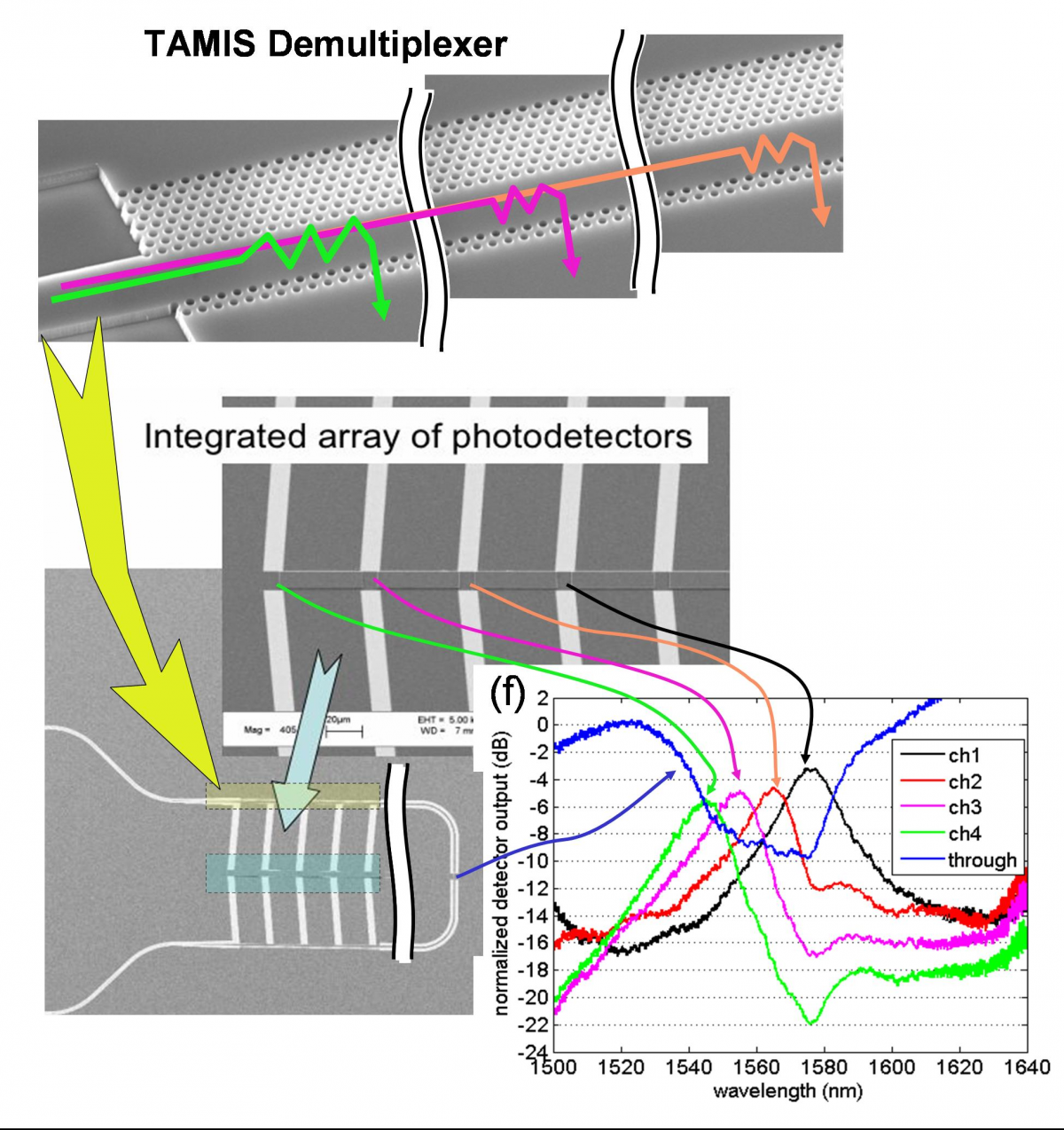
The invention concerns a frequency selective light coupling and decoupling device based on a multimode photonic crystal waveguide. If a signal is injected on its fundamental mode, it is converted into a higher-order mode inside the structure. Then, this higher-order mode is outcoupled without perturbing the fundamental mode by thinning to a few rows the lateral photonic crystal cladding on one side (or both sides). The wave leaks as a local plane wave that can be channelled to the next device on a chip. Multiple channels are implemented at successive locations along the waveguide by simply varying the width of the waveguide (or the axial period of the photonic crystal), once every 10 to 100 crystal periods typically, and possibly by providing short “dead zones” between such sections to celan up the signal. The system may also be used as a combiner (reciprocity) or as a wavelength monitor if photodiodes are implemented monolithically at the selected channel positions, just aside the waveguide.
BENEFITS
For demux applications, this system can compete with microdisks and other in-plane selective elements. One advantage is the structural integrity, there is no full gap to etch between guide and disk. It can also operate at modest Q (~50-200), which is difficult for microdisks. Once the crystal hole size is mastered, the series of demultiplexed wavelength can be chosen at will with great accuracy and in any order, which is also an advantage on PHASAR. Signals at non-dropped wavelengths are virtually unaffected. The implementation can be quite compact, 5×30 micron for coarse WDM channels, per channel, hence 5×240 micron for an N=8 channel function (ie the same area than N typical 5×30 µm photodiodes). It works equally well on InP, GaAs and SoI cases, and could also be used at mid infrared wavelengths down to THz systems. The picture below shows the implementation made on SoI in a polrisation-diversity demux chip, in the framework of the EU IST FUNFOX 04582 FP6 project, notably with collaboration from Ghent University (with IMEC) and St Andr’ews university for these particular realisations. The device is nicknamed “TAMIS demultiplexer” Tamis being the French for “sieve”.

INDUSTRIAL APPLICATIONS
This device can be used for demultiplexing. The output wavefront is not optimized in the standard version, so that dropping the signal to photodiodes is a preferred option to make good use of the device according to the invention. However, focussing structures can be envisioned.
It can be used for wavelength monitoring “online” by dropping channels to the device (or only part thereof). It can also be used to stabilize the wavelength of a tuneable laser, by providing sufficient data for proper feedback [4].
Applications can be on InP, GaAs or SoI substrates, or even other systems.
ADDITIONAL INFORMATION
Selected publications on this topic illustrates the design, operation, and critical fabrication parameters:
[1] E. Viasnoff-Schwoob, C. Weisbuch, H. Benisty, C. Cuisin, E. Derouin, O. Drisse, G.-H. Duan, L. Legouézigou, O. Legouézigou, F. Pommereau, S. Golka, H. Heidrich, H. J. Hensel, and K. Janiak, « Compact wavelength monitoring by lateral outcoupling in wedged photonic crystal multimode waveguides, » Appl. Phys. Lett., vol. 86, pp. 101107, 2005.
[2] L. Martinelli, H. Benisty, O. Drisse, E. Derouin, F. Pommereau, O. Legouézigou, and G. H. Duan, « Impact of Lithographic Grid Irregularity Assessed on Photonic Crystal Device Selectivity, » IEEE Phot. Technol. Lett., vol. 19, pp. 282-284, 2007.
[3] L. Martinelli, H. Benisty, O. Khayam, G. H. Duan, H. Heidrich, and K. Janiak, « Analysis and optimization of compact demultiplexer monitor based on photonic crystal waveguide, » IEEE J. Lightwave Technol., vol. 25, pp. 2385-2394, 2007.
[4] H. Hofmann, M. Kamp, A. Forchel et al., A. Forchel, D. F. G. Gallagher, and H. Benisty, « Integrated wavelength monitoring in a photonic-crystal tunable laser diode, » Photonics and Nanostructures, Fundamentals and Applications, vol. 6, pp. 205–212, 2008.
[5] T. Stomeo, F. Van Laere, M. Ayre, C. Cambournac, H. Benisty, D. Van Thourhout, R. Baets, and T. F. Krauss, « Integration of grating couplers with a compact photonic crystal demultiplexer on an InP membrane, » Optics Lett., vol. 33, pp. 884-886, 2008.
[6] F. Van Laere, D. Van Thourhout, R. Baets, T. Stomeo, T. F. Krauss, M. Ayre, C. Cambournac, and H. Benisty, « Multifunctional Photonic Crystal Compact Demux-Detector on InP, paper OThM5, » presented at OFC/NFOEC 2008, 25-28 Feb., San Diego, 2008.
A paper was also accepted in J. Lightwave Technol. (probably to appear in 2009), based on this communication.
[7] Grating coupled Photonic Crystal demultiplexer with integrated detectors on InP membrane
F. Van Laere, T. Stomeo, M. Ayre, C. Cambournac, R. Brenot, D. Van Thourhout, H. Benisty, T.F. Krauss, R. Baets,
Indium Phosphide and Related Materials Conference, Versailles, Mai 25-29, paper MoB3.4 (2008).
[8] Functional photonic-crystal mini-stopband demux integrated in emitting and detecting
devices
H. Benisty, C. Cambournac, M. Ayre, F. Van Laere, D. Van Thourhout, R. Baets, T. Stomeo3, T.F. Krauss, M.Kamp, H. Hoffman, A. Forchel, D.F.G. Gallagher
14th European Conference on Integrated Optics ECIO’08, Eindhoven (Pays-Bas), June 11-13, paper ThC2 (2008).
For further information, please contact us (Ref 86031-01)